EN
EN

Printed Electronics for Flexible Sensors | VMANX
VMANX, an ISO 9001-certified printed electronics manufacturer founded in 2006, develops printed electronics for flexible sensors in Dongguan, China, for industrial controls, smart appliances, robotics and thin human-machine interfaces. The process deposits silver, carbon and dielectric inks directly onto PET, PI or functional polymer films, because the circuit must bend, fit a restricted envelope and often sense force, touch, position or vibration on the same surface. By combining pattern printing, controlled curing, lamination, die-cutting and electrical testing, one thin-film component can replace separate wiring, switches and sensing elements.
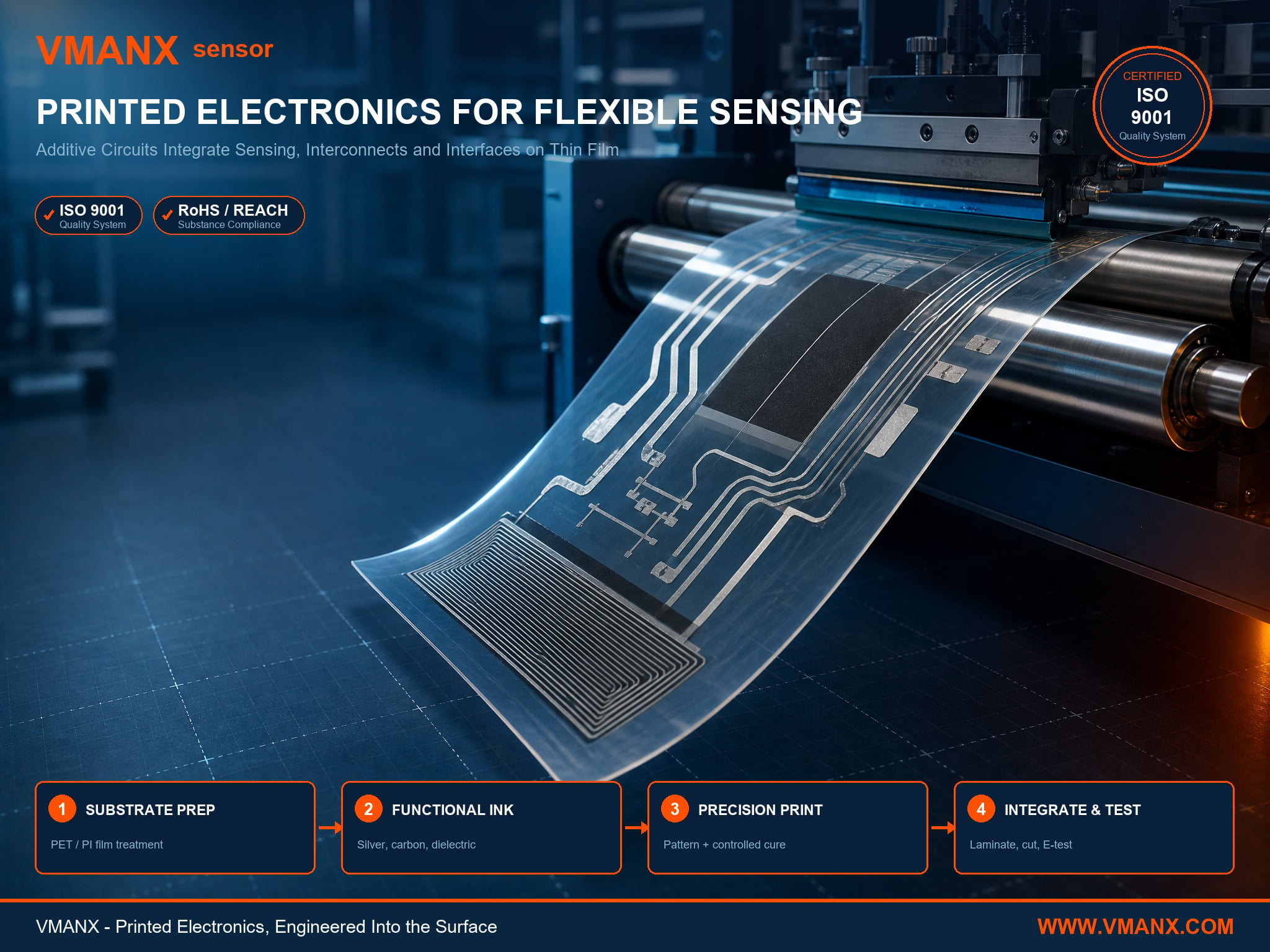
A Circuit Can Become Part of the Surface
Conventional electronics begins with a rigid board and asks the product to make space for it. Printed electronics begins with the product surface and asks which electrical functions can be built into that geometry.
A conductive pattern can become an interconnect. Carbon ink can form a resistive element. A printed electrode can collect a biological or piezoelectric signal. A dielectric layer can let two circuits cross without shorting. Metal domes, LEDs and connectors can then be integrated where the interface requires physical feedback or illumination.
The result is not simply a thinner circuit board. It is a different architecture: the sensing layer, wiring and user interface can share one flexible carrier instead of being assembled as separate mechanical parts.
Key Features & Benefits Additive Patterning Uses Material Only Where Function Is Needed
In a silver-printed PET circuit, conductive paste is deposited only where a trace, electrode or contact is required. The official VMX-FPC-AG process follows PET cutting and corona treatment with silver printing, thermal curing, optional dielectric or carbon printing, low-temperature stiffener lamination, cutting and electrical testing.
This additive route avoids the full copper-removal sequence used in etched circuitry. For low-current signal paths and simple one- or two-layer designs, that means faster prototyping and lower volume cost without paying for performance the application does not use.
Functional Inks Turn One Film Into Several Components
Printed electronics is valuable because each ink performs a different electrical job:
• Silver paste forms low-resistance conductors and contact pads.
• Carbon ink forms resistive tracks and force-sensitive zones.
• Dielectric ink insulates crossing conductors and protects selected regions.
• Printed electrodes couple mechanical, touch or piezoelectric input into the circuit.
Layering these materials on one substrate lets an engineer create a pressure sensor, membrane potentiometer, touch interface or signal pickup without adding a separate wire harness for every function.
Flexible Substrates Fit Where Rigid Boards Cannot
PET is available in 50, 75, 100, 188 and 250 μm thicknesses, including transparent options. PI substrates are available from 12.5 to 125 μm where higher temperature, tighter geometry or SMT assembly is required. PVDF film adds an active piezoelectric layer for vibration, acoustic and dynamic-force sensing.
These films can wrap around curves, run under overlays, pass through narrow housings and remain hidden inside a finished product. The circuit is designed around the mechanical envelope rather than forcing the enclosure around a board.
Printed Electronics Supports More Than One Sensor Physics
The same manufacturing platform serves several electrical behaviours:
• Piezoresistive FSR converts applied force into a resistance change.
• Capacitive touch detects proximity or finger interaction through an overlay.
• Membrane potentiometry converts linear or rotary position into an analogue output.
• PVDF piezoelectric film converts dynamic force, vibration or acoustic energy into charge.
• Membrane switching combines printed circuits with tactile domes, overlays and optional illumination.
This matters to OEM teams because one supplier can solve several interfaces with related materials, tooling and inspection logic rather than introducing a separate manufacturing chain for every sensing modality.
Three Material Platforms, Three Engineering Windows
Printed electronics is not one universal material stack. The correct platform depends on temperature, current, bend life, optical requirement and assembly method.
PET Silver-Printed Circuits — Fast, Thin and Potentially Transparent
VMX-FPC-AG uses screen-printed silver paste on PET. Standard silver dry thickness is 5–15 μm, minimum line/space is 150/150 μm with 100/100 μm available through an advanced process, and current capacity is up to 0.8 A under the stated trace condition. The operating window is -20°C to +80°C with more than 50,000 flex cycles.
Its differentiator is optical freedom: the optional AgNW version reaches at least 89% transmittance at 550 nm with sheet resistance of 50–100 Ω/sq. That makes the platform suitable for transparent touch, low-power sensors, LED strips and rapid prototypes. The trade-off is equally clear: PET is not reflow-solderable and component attachment must use a low-temperature conductive adhesive.
PI Copper FPC — Precision, Current and SMT Compatibility
VMX-FPC-CU uses etched copper foil on PI. It supports 75/75 μm minimum line/space, 50/50 μm with 0.5 oz copper, controlled impedance of 50 Ω single-ended or 100 Ω differential at ±10%, and more than 200,000 flex cycles with RA copper under the stated test method. The operating range extends from -40°C to +150°C, and the construction supports reflow soldering.
This platform is the correct choice when the circuit carries higher current, needs dense component placement, must survive repeated dynamic bending or must hold controlled impedance. It is not the lowest-cost answer, but it buys electrical and assembly headroom the silver-printed route cannot provide.
PVDF Printed Electrodes — The Film Itself Becomes the Sensor
The VV-PVDF6866 platform uses high-purity PVDF film with printed silver-paste electrodes and multilayer encapsulation. Core film is available at 28, 44 and 110 μm; the electrode layer is 5–10 μm thick. Published performance includes a 0.1 Hz–100 MHz frequency response, ±1% full-scale linearity error, -20°C to +85°C operation and a dielectric breakdown voltage of at least 1800 VDC for 44 μm film.
Here the printed electrode is not merely carrying a signal from a separate sensor — it is collecting charge from the active film itself. That allows thin, conformable vibration, acoustic and dynamic-force sensors for equipment monitoring, transportation, medical-device development and wearable feedback.
Technical Specifications
| Platform | Substrate / Active Film | Conductive Layer | Key Verified Performance | Assembly / Best Fit |
| VMX-FPC-AG | PET 50/75/100/188/250 μm | Printed silver, 5–15 μm dry | 150/150 μm line-space; ≤0.8 A; >50,000 flex cycles; -20°C to +80°C | Conductive adhesive; low-current sensors, transparent touch, rapid prototypes |
| VMX-FPC-CU | PI 12.5/25/50/125 μm | Etched copper 18/35/70 μm | 75/75 μm line-space; 50/50 μm advanced; >200,000 cycles; -40°C to +150°C | SMT/reflow; dense interconnects, higher current, controlled impedance |
| AgNW Transparent | Transparent PET | Silver nanowire | 50–100 Ω/sq; ≥89% transmittance at 550 nm | Transparent touch and optical interfaces |
| VV-PVDF6866 | PVDF 28/44/110 μm | Dual-side silver paste, 5–10 μm | 0.1 Hz–100 MHz; ±1% F.S.; ≥1800 VDC breakdown; -20°C to +85°C | Vibration, acoustic and dynamic-force sensing |
| Membrane Switch | Flexible printed circuit stack | Silver/carbon/dielectric ink options | Ultra-thin HMI construction; configurable tactile and illuminated interface | Industrial controls, smart appliances and sealed user interfaces |
Values are product-platform specifications published by VMANX, not universal limits for every printed-electronics design. Final performance depends on geometry, ink, substrate, cure profile and integration method.
The Manufacturing Chain That Determines Repeatability 1. Substrate Preparation
Film arrives as a mechanical material, not an electronic component. Cleaning, cutting and surface treatment determine whether functional ink wets and bonds consistently. PET silver circuits use corona treatment before printing; an under-treated surface may look acceptable at first inspection while failing later under flex or humidity.
2. Functional Ink Deposition
Screen or precision pattern printing defines the conductive and sensing geometry. Trace width, dried-film thickness and registration control resistance and channel-to-channel consistency. A low-cost ink deposited inconsistently is not a low-cost circuit — it is a variable resistor disguised as wiring.
3. Controlled Curing and Layer Build
Cure energy determines whether printed silver achieves the intended conductivity and adhesion. Optional carbon and dielectric layers add sensing or insulation functions, but each new layer introduces registration and cure-stack interactions that must be validated as a system.
4. Lamination, Cutting and Electrical Test
Protective layers, stiffeners, adhesive systems and connectors are added before final die-cutting. Electrical testing then checks continuity, isolation and the relevant sensor response. This is where a printed pattern becomes a controlled component rather than decorated film.
When Printed Electronics Is the Wrong Choice
Printed electronics wins when geometry, thinness, flexibility, transparency or integrated sensing matters more than maximum conductor density and power handling. It is not automatically the best answer for every circuit.
If the product requires dense SMT population, repeated high-temperature reflow, controlled impedance or current above the silver platform's thermal limit, PI copper FPC is the stronger choice. If it requires low-frequency static weight measurement at laboratory accuracy, a load cell may be more appropriate than an FSR. If the requirement is room-level presence rather than pressure on one surface, radar may fit better than a sensor mat.
The engineering advantage is not forcing every project onto one technology. It is selecting the lowest-complexity platform that still meets the real requirement.
Customer FAQs
Q: What is printed electronics? A: Printed electronics deposits conductive, resistive, dielectric or active materials in patterns on a substrate such as PET, PI or PVDF. The printed layers create circuits, electrodes and sensing zones directly on the film.
Q: Is a printed silver circuit the same as a copper FPC? A: No. Printed silver on PET is an additive, low-temperature process suited to low-current, fast-turn and transparent designs. Copper FPC uses subtractive etching on PI and supports tighter traces, higher current, SMT reflow and controlled impedance.
Q: Can printed electronics be transparent? A: Yes. VMANX's AgNW transparent option publishes 50–100 Ω/sq sheet resistance and at least 89% transmittance at 550 nm. Standard printed silver is visible; transparency requires the dedicated AgNW construction.
Q: Can components be mounted directly on PET silver circuits? A: Yes, but not by standard high-temperature reflow. PET components use low-temperature conductive adhesive. Applications requiring conventional SMT reflow should use the PI copper platform.
Q: How flexible are the circuits? A: The published PET silver platform exceeds 50,000 flex cycles under the stated MIT test, while PI copper with RA copper exceeds 200,000 cycles. Actual life depends on bend radius, stack thickness, trace direction and assembly strain relief.
Q: Which inks are used in a printed sensor? A: Silver ink forms conductive paths, carbon can form resistive or force-sensitive elements, and dielectric ink provides insulation and protection. The exact stack depends on the sensing principle and electrical target.
Q: What certification applies to this industrial printed-electronics platform? A: VMANX manufactures the industrial platform under ISO 9001 with RoHS and REACH substance compliance. Product-specific approvals depend on the final application and are held by the brand placing the finished product on the market.
Q: Can one project combine printed sensors and copper FPC? A: Yes. A hybrid architecture can use printed film for a large-area sensing or touch layer and PI copper FPC for dense components, power and connector routing. The interface between the two must be designed for resistance, strain relief and the chosen assembly temperature.
OEM Engineering Support
VMANX supports printed-electronics programs from material and process selection through circuit layout, prototype and production release. The industrial portfolio includes flexible printed circuits, force sensing resistors, membrane potentiometers, HMI systems and PVDF piezoelectric sensors. Detailed engineering data is available for the two-series industrial FPC platform, industrial thin-film FSR, PVDF film sensor and membrane switch specification.
Conclusion
Printed electronics removes the border between circuit and surface. Conductors, resistors, electrodes, insulation and interface functions can be patterned directly onto flexible films, then laminated, cut and tested as one engineered component. The commercial value is not thinness alone — it is fewer separate parts, less mechanical volume and a sensing architecture shaped to the product instead of forcing the product around a rigid board.